We reach more than 65,000 registered users in Dec!! Register Now
Quantum spin Hall effect in magnetic graphene
- July 04, 2025
- 3 Views
- 0 Likes
- 0 Comment
Introduction
Decades of research in graphene have unveiled its remarkable charge and spin-related properties, such as distinctive quantum Hall (QH) charge transport and long-distance spin propagation1,2. Yet, harnessing topologically protected spin transport for the development of practical quantum spintronic devices necessitates targeted modifications to the graphene band structure. This band structure engineering has been recently achieved non-invasively by bringing graphene in the proximity of other two-dimensional (2D) materials3, leading to spin Hall4,5, Rashba-Edelstein6,7,8, anomalous Hall (AH)9, and spin-dependent Seebeck10 effects in graphene. The realization of these phenomena in proximitized graphene is due to induced spin-orbit and/or exchange interactions that result in spin-splitting of the graphene band structure11,12,13. These spin-related effects, however, have been experimentally addressed in proximitized graphene majorly by diffusive charge/spin transport, where the spin relaxation length is limited by spin and momentum scattering mechanisms. On the contrary, if the transport occurs through topological spin-polarized edge states, their topological protection allows for long-distance quantum coherent spin propagation.Spin-polarized chiral and helical QH edge states have been detected in graphene through the Zeeman splitting of the bands by applying large magnetic fields14,15,16, which is conceived to be practically challenging for applications. Thus, numerous theoretical and experimental reports so far focus on resolving spin-polarized edge states in graphene without the need for any external magnetic field, possible through the emergence of quantum spin Hall (QSH) or quantum anomalous Hall (QAH) states in a modified graphene band structure17,18,19,20,21,22,23,24,25,26,27,28. These spin-polarized gapless edge states can form within the bulk gap of graphene, attainable by inducing staggered potentials, spin-orbit coupling (SOC) and/or magnetic exchange interactions17,18,19. Depending on the respective magnitude of the spin-orbit vs. exchange interactions, these edge states can be chiral or helical20, allowing for topologically protected spin transport that is expected to be robust against disorder18.
Despite several recent experimental efforts in addressing the topological transport in various graphene-based van der Waals heterostructures29,30,31,32,33,34, direct experimental evidence for the detection of the QAH and QSH effects in proximitized graphene is still missing. One major obstacle has been the presence of dominant interfacial charge transfer35,36 that may hinder the exploration of the proximity effects. In this work, however, the suppression of the interfacial charge transfer in graphene-CrPS4 heterostructures allows us to study the transport in the presence of magnetic exchange and spin-orbit interactions, evidenced by the detection of a large AH signal up to room temperature. Remarkably, we experimentally realize the presence of helical states at zero external magnetic field, indicating the emergence of the QSH effect despite the breaking of time-reversal symmetry by the induced magnetism20,37. The unprecedented zero-magnetic-field detection of the QSH state in this graphene-based magnetic heterostructure, coexisting with the AH effect, makes this system intriguing for the development of quantum spintronic circuitries.
Results
We bring graphene in the van der Waals proximity of the interlayer antiferromagnet, CrPS4 (CPS), which is an air-stable semiconductor with a bandgap of ~1.3 eV38 and a Néel temperature TN ≈ 38 K39. Figure 1a (top panel) illustrates a top view of the CPS crystal structure with the dashed lines indicating the crystallographic directions along which the crystals preferentially cleave, as shown in the optical micrograph of an exfoliated flake. As a result, the CPS flakes acquire a corner angle of 67.5°, the bisector of which is along the magnetic a-axis38 (see also supplementary information (SI), Figure S2). The presence of this characteristic angle assists with the identification of the CPS crystallographic orientation and guides the alignment of the graphene Hall bar with one of the CPS magnetic axes (see Figure 1a, lower panel). In accordance with previous reports39, CPS has an anisotropic magnetic behavior which is evaluated using a superconducting quantum interference device (SQUID) at various temperatures (T), shown in Fig. 1b and c (see Methods for more details on CPS). The SQUID measurements at the small-range Bz (panel b) for T < 40 K show the expected spin-flop transition when the magnetization of the layers rotates from canted out-of-plane towards the in-plane b-axis, while holding their respective antiparallel alignment (lower inset in Fig. 1b). Increasing Bz above the spin-flop transition field (Bsf ~ 0.8 T at 2 K) results in canting of the magnetic moments towards the c-axis, starting with ~6° canting (upper inset in panel b) until full saturation (90°) at Bz ≈ 8 T, as shown in Fig. 1c.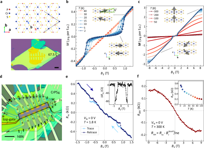 a Top-view (a − b plane) schematic of monoclinic CPS crystal structure (space group C251). The optical micrograph (scale bar: 10 μm) shows a 38 nm thick CPS flake covered with an hBN/graphene Hall-bar (see SI, Figure S1). b, c SQUID magnetometry of a CPS bulk crystal at various temperatures (T) for small (b) and large (c) range of magnetic field Bz, applied perpendicular to the (a − b) plane. The Bz cycling shows a minimal hysteresis in CPS bulk magnetization. Insets: side-view schematics of CPS layers magnetic ordering at indicated Bz ranges. d Optical micrograph of device A fabricated with an hBN/graphene/CPS heterostructure on a SiO2/Si substrate with Ti-Pd electrodes. Scale bar: 10 μm. The hBN and SiO2 layers, used as top- and back-gate dielectrics, are 73 and 285 nm thick, respectively. e Transverse resistance Rxy = Vxy/I measured vs. Bz in the graphene Hall-bar at T = 1.8 K with I = 0.5 μA, at back-gate and top-gate voltages of Vbg = 50 V and Vtg = 0 V. The non-linearity of Rxy at Bz < 1 T is due to non-linear CPS magnetization behaviour in that Bz range (see Figure S4). Inset: subtraction of the trace and retrace measurements (ΔRxy), showing the Rxy modulation due to spin-flop transition. The asymmetry in the ΔRxy vs. Bz arises from non-symmetric magnetization behavior of the outmost CPS layer through the spin-flop transition, likely caused by neighboring magnetic domains in the CPS flake. f Non-linear component of Rxy associated with the AH effect (RAH), measured at T = 300 K, Vbg = 50 V and Vtg = 0 V. RAH is acquired by subtraction of a linear background (related to the ordinary Hall effect) from Rxy anti-symmetrized vs. Bz (also see SI Figure S3). For the linear fit, the Rxy data in the range of 8 T < Bz ≤ 9 T is considered, assuming saturation of the magnetization in that range. Inset: Temperature-dependence of RAH at Vtg = 0 V. The RAH is estimated as the lower bound, averaged over the RAH for Bz > 6T (see SI, section 4).
Full size image
The trace and retrace measurements of Rxy in Fig. 1e show no hysteresis vs. Bz, except for Bz close to Bsf. This hysteresis is absent in the SQUID measurements of the bulk crystal, implying the sensitivity of the AH effect to the behaviour of the magnetization of the outer-most layer of the CPS (MCPS). Under applied Bz, the behavior of MCPS is expected to be ruled by its antiferromagnetic coupling with respect to the other CPS layers, and yet, the lack of a neighboring CPS layer on top can cause the MCPS to lag behind the magnetization dynamics of the bulk of CPS, leading to the observed hysteresis. By decreasing Bz, MCPS undergoes a spin-flop transition at ~0.5 T, by which Rxy in the retrace retrieves its initial value as in the trace measurement. The difference of Rxy in the trace and retrace measurements is about 80 Ω (shown in the inset of Fig. 1e), which is the AH effect signal generated by the spin-flop transition of the MCPS.
The AH resistance (RAH) is dependent on the projection of the magnetization MCPS along the c-axis. From the comparison of the magnetization values measured by SQUID at Bz ~ 0.8 and 8 T (in Fig. 1c), one can tell that through the spin-flop transition, the MCPS cants towards the c-axis only by 6 degrees, which has led to RAH ≈ 80 Ω. Considering that and the linear relation between the RAH and z-component of MCPS, RAH should be about 700 Ω when MCPS is fully saturated out-of-plane, consistent with the value we measure at large Bz (see SI, Figure S5). Further evaluation of the AH effect at various temperatures is shown in Fig. 1f (inset), indicating a considerable decay vs. T. Yet, there is a finite value of RAH of about 150 Ω that persists up to 300 K. Note that at elevated temperatures CPS is a paramagnet, thus a finite magnetic field is required to induce magnetism in graphene. The detected RAH in this heterostructure is larger than that achieved so far in proximitized graphene9,10,40,41. The observation of such a sizable RAH is a signature of the co-presence of strong induced spin-orbit and exchange interactions42 in the proximitized graphene up to room temperature, which is consistent with the recently reported enhancement of the Curie temperature at the graphene-CPS interface43. The detection of the unprecedentedly large AH effect in this system is also expected from the strong hybridization between the graphene and CPS bands, shown by our density functional theory (DFT) calculations (see SI, Section 14).
Having established the proximity-induced magnetism in the graphene channel, we explore the QH regime of transport in this system. By cooling down the device, signatures of QH transport become evident at finite Bz, as shown in Fig. 2. Panel a shows the modulation of the longitudinal resistivity (ρxx) vs. Bz, i.e., the Shubnikov de-Haas oscillations (SdHOs). The back-gate voltage (Vbg) is set to 50 V to shift the Dirac point such that the electron-like Landau levels (LLs) are reachable by the top-gating. We evaluate the back-gate vs. top-gate dependence of the LLs in Figure S7, indicating only a shift of the LLs by electrostatic doping without any significant change in the Landau fan diagram with Vbg (SI, Figure S8). Moreover, there is a negligible shift of the Dirac peak vs. Bz (SI, Figure S9) and there is a minimal hysteresis for the Vtg-dependence of ρxx, which decreases with raising temperature (SI, Figure S10). These observations are in contrast with recent reports on graphene in the proximity of CrX336 or CrOCl35, where gate-dependent interfacial charge transfer influences the transport in graphene.
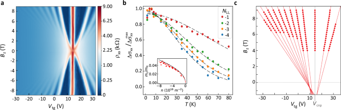 a Shubnikov-de Haas oscillations of the longitudinal resistivity ρxx in graphene, measured vs. applied top-gate voltage and magnetic field (using voltage probes V5 and V6, shown in Fig. 1d). b Amplitude of the SdHOs (Δσxx) for LL number of NLL = − 1 to −4 as a function of T, normalized to their maxima. Dashed lines are the fits to the data using Δσxx=T/sinh(2π2kBTmc/ℏeBz). Inset: cyclotron mass, mc, extracted from all the hole-like LLs, plotted as the ratio with respect to the electron rest mass (m0) vs. carrier density (n). The red curve is a fit to the extracted mc/m0 vs. n, considering a linear dispersion relation, resulting in Fermi velocity, vF ≈ 1.196 × 10⁶ m/s. The black curve is the theoretically expected behavior for pristine graphene with vF = 1.1 × 10⁶ m/s. The effective n in the graphene channel is extracted from Hall measurements (for Bz ≥ 8 T), and separately from the dependence of Bz vs. Vtg for each LL. These two approaches give rise to similar extracted values for n (see SI, Section 8). c Landau fan diagram: the red dots are the maxima of the ρxx vs. Vtg extracted from panel a for gate voltages slightly away from the charge neutrality point (∣Vtg − Vcnp∣ > 5 V), with the red dashed lines as linear fits.
Full size image
However, the Landau fan diagram in graphene-CPS (Fig. 2a) differs from that of pristine graphene, showing shifts of the LLs in Vtg and minimal broadening of the zeroth LL (zLL) vs. Bz. A slight non-linearity of the first Landau fans is present close to zero energy which could be related to a small non-linear dependence of n vs. Vtg close to the charge neutrality point (Vcnp). This nonlinearity is likely related to a small contribution of CPS localized midgap states in the total capacitance at low density of states in graphene, particularly at large positive Vtg when the Fermi energy EF is expected to get closer to the conduction band edge in the CPS. In Fig. 2c, we show the maxima of ρxx vs. Vtg for ∣Vtg − Vcnp∣ > 5 V, together with the linear fits, clearly showing the linear behavior of the Landau fans. That also rules out the dominant contribution of interfacial charge transfer that would cause nonlinearities in Landau fans due to its dependence on magnetic ordering35,36. Figure 2c further indicates that the Landau fans do not converge at one point at Vcnp, implying finite shifts of the LLs in Vtg. We can correlate the shift of the LLs to the opening of the bulk gap at the charge neutrality point in the graphene channel due to the induced staggered potential. The shift is pronounced in the Vtg-dependence since the presence of the CPS midgap states within the graphene bulk gap and LL gaps slows down the tuning of the EF close to the Vcnp (further details in SI, Section 9). It is also worth noting that the zLL shows minimal broadening and a negligible increase in resistance vs. Bz, in contrast to that reported in pristine graphene14. This observation is suggestive of the presence of edge states at the zLL gap that shunt the transport at Vcnp. The slow modulation of the EF by Vtg within the zLL energy gap in this system can assist with resolving the edge states within the gap.
On another note, we highlight that the spin-splitting of the LLs with NLL ≠ 0 is not resolved within the broadening of the SdHOs in the Landau fan diagram of Fig. 2a. We attribute this to the presence of disorder in this system (with low charge carrier mobility), hindering the resolution of the spin-split bands at higher energies. In fact, the absence of the spin-split Landau fan diagram indicates that the induced magnetism is not large in this heterostructure, and thus the observation of the strong AH effect should be mainly due to a sizable SOC induced in the graphene channel. The larger induced SOC, as compared with the exchange interaction, is expected to result in the emergence of helical (and not chiral) states in this heterostructure20. In fact, depending on the relative strengths of Rashba SOC, Kane-Mele SOC, and magnetic exchange interactions, the system can transition between the QSH and QAH regimes20.
For addressing the topological edge states in the graphene bulk gap, we focus on the transport close to zero energy. Helical states are spin-polarized electron- and hole-like bands within the bulk gap of the proximitized graphene18 that counter-propagate at the edges of the graphene channel, as shown in the schematics of Fig. 3a. Figure 3b shows the gate-dependence of the graphene resistivity (ρxx, left axis) and resistance (Rxx, right axis) close to the charge neutrality point, for small applied magnetic fields (Bz ≤ 0.5 T). The ρxx shows oscillations that develop into the SdHOs in the Landau fan diagram of Fig. 2a at higher Bz. The Vtg dependence of ρxx at Bz = 0 T (in Fig. 3b) has a wide peak at the charge neutrality point. When such four-terminal longitudinal measurements are evaluated in terms of conductance (G = 1/Rxx = I/Vxx), as shown in Fig. 3c for different voltage probe pairs, it becomes evident that the broadened resistance peak at Vcnp at 0 T is a plateau of conductance at 2 e2/h. This quantized conductance at zero energy is evidence for the presence of counter-propagating spin-polarized helical states, as depicted in Fig. 3a.
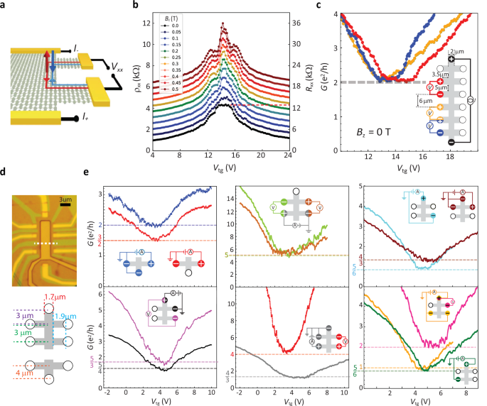 a A schematic of the device and a four-terminal measurement geometry are shown with the propagation direction of the helical states at the edge of the graphene channel. b Vtg-dependence of the graphene resistivity, ρxx, (left axis), and resistance, Rxx (right axis), at Bz = 0 to 0.5 T. The measurements are performed using the first voltage pair as in Fig. 2a. The plots are offset (except for Bz = 0 T) for a clearer visualization of the SdHOs. The red dashed line is to highlight the value of the Rxx ≈ 13 kΩ at the charge neutrality point. c Conductance (G = I/Vxx) vs. Vtg close to the charge neutrality point at Bz = 0 T, measured in the four-terminal configurations shown in the schematics of the device in the inset (the graphene channel length and width are 6 and 2 μm, respectively). d Optical micrograph and schematics of device C that has two separate graphene channels with a different aspect ratio compared with that of devices A and B (the dimensions of the graphene channels are indicated in the schematics). The white dashed line in the optical image indicates the position where the graphene channel is cut to form two electrically isolated regions with 3 and 5 electrodes. e Two-, three- and four-terminal conductance in device C, measured at various configurations shown in the schematics of the device in the insets. Note that the VCNP in device C is around 4–6 V. All measurements are performed at Bz = 0 T at T = 2.3 K. The dashed lines indicate the theoretically expected values for conductance considering helical states, color-coded with respect to the measurement geometry indicated in the inset.
Full size image
G2T=e2h(1NL+1+1NR+1),(1)where NL and NR are the number of floating probes between the source and drain, along the left and right edges of the conductor. Similarly, the four-terminal conductance G4T is given by
G4T=G2TNI+1NV+1,(2)where NI is the number of floating probes in between the source and drain along the edge which hosts the voltage probes, and NV is the number of floating electrodes in between the voltage probes48. For the measurement of Fig. 3c, NL = NR = NI = 6, and NV = 0, thus, G4T = 2 e2/h, which is the value measured at Bz = 0 T at the zLL conductance plateau. Considering the equations above, we evaluate the transport in various two-, three- and four-terminal measurement geometries, shown for device A in the SI, Figure S20, and for device C in Fig. 3e. The graphene channel in device C has been cut by an atomic force microscope tip, shaped into the Hall bar geometry with an aspect ratio different from that of device A and B, to rule out any coincidental geometrical factors in the measured conductance. Device C consists of two electrically disconnected regions with three and five electrodes connected to the channel (Fig. 3d). In panel e, the expected G values considering the helical edge states, following equations 1 and 2, are shown by the dashed lines that are color-coded with respect to each measurement geometry. We observe that, despite the distinct G measured at Vtg ≠ Vcnp, the conductance values at Vcnp in each geometry closely match the theoretical values expected in the presence of QSH effect, confirming that the helical states dominate the charge transport at Vcnp in the magnetized graphene in the absence of an external magnetic field.
Under finite Bz, the conductance at the charge neutrality point in device A just slightly deviates from the quantized value of 2e2/h, as shown in Fig. 4a. Persistence of helical states at finite Bz depends on the evolution of the zLLs and can be disturbed by bands crossing at certain Bz49. In this case, the temperature dependence of the QH transport can provide further insight into the nature of the zLL gap50. In Fig. 4b, we show the gate-dependence of the graphene resistance at Bz = 9 T up to room temperature. We observe that the resistance at the zLL increases by increasing T. This metallic T-dependence is consistent with the presence of the gapless helical states at the zLL up to large Bz. In the inset of panel b, the T − dependence of Rxx at zero energy is compared for Bz = 0 and 9 T. The slight decay of Rxx vs. T at Bz = 0 can be related to the scattering of the spin-polarized edge states at higher T due to random fluctuations of the magnetic moments (which is eliminated at large Bz). Thus, at Bz = 0 the contribution of the bulk transport becomes more dominant at higher T and the resistance drops as a result of the thermal broadening of the Dirac peak.
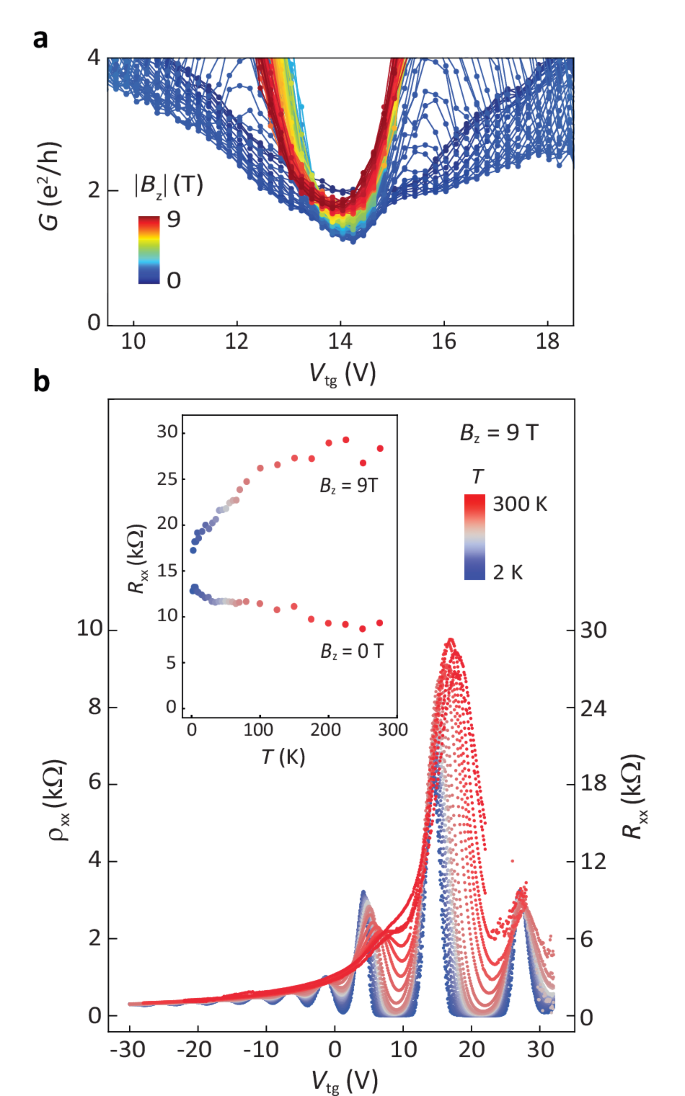 a Vtg-dependence of the conductance close to the Vcnp, measured at 0 < ∣Bz∣ < 9 T in a four-terminal geometry with V5 and V6 voltage probes in device A. b Gate-dependence of the graphene resistivity (left axis) and resistance (right axis) at Bz = 9 T, measured at various T. Inset: Temperature-dependence of the maxima of the four-terminal resistance at Vtg = Vcnp, shown for Bz = 0, 9 T.
Full size image
Methods
CrPS4 Synthesis
CrPS4 crystals are grown following a solid-state reaction. Stoichiometric amounts of Cr (99.99%, Alfa-Aesar), P (>99.99%, Sigma-Aldrich) and S (99.99%, Sigma-Aldrich) are sealed inside an evacuated quartz tube (pressure 5 × 10⁻⁵ mbar, length: 50 cm, internal diameter: 14 mm) and placed in a three-zone furnace. A temperature gradient of 750/650/700 °C is kept for 21 days followed by a quench into water. The obtained crystals are analyzed by powder X-ray diffraction and energy-dispersive X-ray spectroscopy. The refinement of the X-ray pattern (ICSD 25059) reveals a monoclinic C face center crystal system with C121 space group and a unit cell determined by α = γ = 90° and β = 91.99(1)° and a = 10.841(9)Å, b = 7.247(6)Å and c = 6.100(5)Å. The amount of elements is Cr:23.3 ± 0.5%, P:14.8 ± 0.4% and S:61.8 ± 1.5%, in good agreement with the expected ones (Cr:24.6%, P: 14.7% and S: 60.7%). The obtained results are in accordance with the ones previously reported in the literature39. Note that the CPS flakes used in heterostructures with graphene in this work are from the same batch of crystal which is characterized by the SQUID magnetometry in Fig. 1b, c.Electrical characterization
The charge transport measurements are performed using a DC current source, and voltages are measured using Keithley 2100 multimeters. DC voltage source is used for the gates. The measurements are performed using a variable temperature insert at He atmosphere (attoDry2100 system).List of Referenes
Cite This Article as
"Quantum spin Hall effect in magnetic graphene", MachPrinciple, July 04, 2025, https://machprinciple.com/post/Quantum-spin-Hall-effect-in-magnetic-graphene
No tags found for this post